A Practical Map of AI Chips: CPU, GPU, TPU, NPU, LPU, ASIC
A Practical Map of AI Chips: CPU, GPU, TPU, NPU, LPU, ASIC
Summary
In this solo “Attention Span” episode, Ksenia Se sets out to demystify the alphabet soup of AI silicon — CPU, GPU, TPU, NPU, LPU, IPU and more — by drawing a single practical map. Rather than a formal hardware taxonomy, she offers a lens: a spectrum of programmability versus specialization. The governing rule, which she asks viewers to hold for the whole episode, is that the more general a chip is, the more flexible it is but the more energy and time it wastes on overhead for any single task; the more specialized a chip is, the faster and cheaper it runs one task and the more useless it becomes for everything else. Every chip is a point on that line, and much of recent AI hardware history is the industry sliding rightward, one workload at a time.
The tour starts at the flexible far left with the CPU, whose lineage runs back through ENIAC and Von Neumann’s stored-program architecture to Intel’s 4004, and which excels at latency-sensitive branching logic but is a poor fit for the trillions of repeated multiplications that training demands. Next comes NVIDIA’s GPU, which won by pairing thousands of lightweight parallel cores with the CUDA software platform — and the discovery that neural networks, like pixels, are a parallel problem. From there the map moves right into ASICs: Google’s TPU with its systolic array, Cerebras’s dinner-plate-sized wafer-scale engine, AWS Trainium and Inferentia, Groq’s LPU (whose technology NVIDIA licensed in a reported ~$20B deal), and finally Taalas’s Talos chip with the model hard-wired into silicon — the logical endpoint where chip and workload become the same object.
The recurring villain throughout is data movement: for token-by-token inference, shuttling data between memory and processor is often more limiting and energy-hungry than the arithmetic itself, and nearly every chip on the right side of the map is a different attack on that problem. Ksenia rounds out the picture with consumer NPUs (Apple’s Neural Engine, Qualcomm Hexagon), APUs that fuse CPU and GPU around shared memory (AMD MI300A, NVIDIA Grace Hopper), and frontier bets like Graphcore’s IPU, FPGAs, and IBM’s in-memory RPU research. Her conclusion: the era when “AI hardware” meant one chip is closing, and the era of the portfolio — hardware tailored to each stage of the model lifecycle — has begun. When a new three-letter acronym appears, just ask what workload it targets and whether that workload is stable enough to deserve its own silicon.
Highlights
”The more general a chip is, the more flexible it is… the more specialized, the faster and cheaper it runs one task”
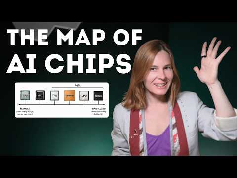
“The more general a chip is, the more flexible it is, and the more energy and time it spends on overhead for any single task. The more specialized the chip is, the faster and cheaper it runs one task and the more useless it becomes for everything else.” — Ksenia Se, 1:35
Clip command
yt-dlp --download-sections "*1:35-1:57" "https://www.youtube.com/watch?v=gTvbNjQtko0" --force-keyframes-at-cuts --merge-output-format mp4 -o "the-one-rule.mp4"”Asking a CPU to do that is asking a brilliant lawyer to hand-address a million mailing requests”
“Training is not one clever thread. Training is the same multiplication repeated trillions of times. And asking a CPU to do that is asking a brilliant lawyer to hand-address a million mailing requests.” — Ksenia Se, 3:39
Clip command
yt-dlp --download-sections "*3:39-4:03" "https://www.youtube.com/watch?v=gTvbNjQtko0" --force-keyframes-at-cuts --merge-output-format mp4 -o "lawyer-mailing-requests.mp4"”It’s usually not the math” — data movement is the real enemy
“It’s usually not the math. Modern chips have compute to spare for many workloads, and especially for token-by-token inference, moving data between memory and processor becomes more limiting and more energy-hungry than the arithmetic itself.” — Ksenia Se, 6:52
Clip command
yt-dlp --download-sections "*6:52-7:17" "https://www.youtube.com/watch?v=gTvbNjQtko0" --force-keyframes-at-cuts --merge-output-format mp4 -o "not-the-math.mp4"Cerebras: a single chip the size of a dinner plate
“Cerebras attacked movement by shrinking the distance. Their wafer-scale engine is a single chip the size of a dinner plate. The WSE-3 carries four trillion transistors, 900,000 cores, and 44 gigabytes of memory living directly on the silicon.” — Ksenia Se, 7:17
Clip command
yt-dlp --download-sections "*7:17-7:51" "https://www.youtube.com/watch?v=gTvbNjQtko0" --force-keyframes-at-cuts --merge-output-format mp4 -o "cerebras-dinner-plate.mp4"Talos: the model physically hard-wired into the silicon
“Talos reports around 17,000 tokens per second per user for its first chip, running a heavily quantized Llama 3.1 8 billion… If you want a different base model, you manufacture a different chip… That is the logical end point of specialization. The chip and the workload become the same object.” — Ksenia Se, 9:27
Clip command
yt-dlp --download-sections "*9:27-10:03" "https://www.youtube.com/watch?v=gTvbNjQtko0" --force-keyframes-at-cuts --merge-output-format mp4 -o "talos-model-in-silicon.mp4"”The era of the portfolio has begun”
“Across the entire axis, the GPU is not going anywhere, but the era when AI hardware meant one chip is closing and the era of the portfolio has begun.” — Ksenia Se, 15:00
Clip command
yt-dlp --download-sections "*15:00-15:27" "https://www.youtube.com/watch?v=gTvbNjQtko0" --force-keyframes-at-cuts --merge-output-format mp4 -o "era-of-the-portfolio.mp4"Key Points
- The map is a lens, not a taxonomy (0:59) - It plots chips on a spectrum of programmability versus specialization, the lens that predicts why designs exist and which one wins where.
- The one rule (1:35) - General = flexible but high overhead; specialized = fast and cheap for one task, useless for everything else. Recent AI history is the industry sliding rightward, one workload at a time.
- CPU lineage (1:57) - Runs back to ENIAC (1945/1946, ~18,000 vacuum tubes), Von Neumann’s stored-program EDVAC report, and Intel’s 4004 (1971), which put an entire CPU on a single chip.
- What defines a CPU (3:05) - Relatively powerful general-purpose cores optimized for latency-sensitive branching logic — a few in a laptop up to nearly 200 in a server socket.
- Why CPUs fail at training (3:39) - Training is the same multiplication repeated trillions of times, not one clever thread.
- GPU origins (4:07) - The modern category crystallized with NVIDIA’s GeForce 256 (1999); pixels are a parallel problem, so a GPU carries thousands of lightweight cores.
- The parallel discovery (4:39) - Neural networks are mostly matrix multiplication, which splits beautifully across thousands of cores. CUDA opened GPUs to general-purpose programming.
- GPU hardware generations (5:01) - V100 (Tensor Cores, 2017) → A100 → H100 → Blackwell / GB200 superchip: the same parallel idea scaled relentlessly.
- TPU and the ASIC question (5:37) - Around 2013 Google asked “what if we stop being general at all?”; the TPU (deployed 2015, revealed 2016) is an application-specific integrated circuit built on a 256×256 systolic array.
- 30–80× performance per watt (6:29) - Google’s 2017 paper showed the TPU beating the contemporary CPUs and GPUs it was benchmarked against, on inference.
- The real enemy is data movement (6:52) - For token-by-token inference, moving data between memory and processor is more limiting and energy-hungry than the math itself.
- Cerebras shrinks the distance (7:17) - WSE-3: four trillion transistors, 900,000 cores, 44 GB of on-silicon memory; the company has since gone public in one of the largest semiconductor IPOs on record.
- AWS Trainium and Inferentia (8:04) - Specialized silicon isn’t inference-only; a cloud provider designing its own training chips keeps the margin it used to pay NVIDIA.
- Groq’s LPU (8:22) - Deterministic execution, compiler control, weights from on-chip SRAM; NVIDIA licensed the tech in a reported ~$20B deal and much of the team, including founder Jonathan Ross, joined NVIDIA.
- LPX rack division of labor (9:00) - 256 LPUs sit beside Rubin GPUs: Rubin handles prefill and attention over large context; LPUs accelerate the latency-sensitive decode loop (feed-forward and MoE from SRAM).
- Talos: model baked into silicon (9:27) - ~17,000 tokens/sec/user on a quantized Llama 3.1 8B; a different base model means a different chip. The endpoint of specialization.
- NPUs in consumer devices (10:13) - Apple’s Neural Engine (A11 Bionic, 2017), Qualcomm Hexagon, Intel/AMD laptop NPUs (AMD’s latest reach ~55 TOPS); optimized for inference at minimal power.
- APUs fuse CPU and GPU (11:20) - AMD’s MI300A (24 Zen 4 cores + 228 GPU compute units + 128 GB unified HBM3) and NVIDIA’s Grace Hopper (NVLink-C2C) eliminate explicit copies between processors.
- Frontier bets: IPU, FPGA, RPU (12:08) - Graphcore’s IPU (1,472 cores), reconfigurable FPGAs, and IBM’s resistive in-memory RPU (2023 64-core analog chip) that computes where the data sits.
- The portfolio conclusion (13:23) - Evolving workloads favor general hardware; predictable, large-scale workloads reward specialization — the same pattern seen in video decoding, cryptography, and Bitcoin mining.
Mentions
Companies
- NVIDIA (4:03) - Creator of the GPU and CUDA; licensed Groq’s LPU tech (~$20B) and now ships a mixed Vera-Rubin platform.
- Intel (2:46) - The 4004 (1971) put an entire CPU on a single chip; also builds NPUs into laptop processors.
- Google (5:37) - Designed the TPU starting ~2013, deployed 2015, revealed 2016; published the 2017 performance-per-watt paper.
- Cerebras (7:17) - Wafer-scale engine (WSE-3); recently went public in one of the largest semiconductor IPOs on record.
- AWS (8:04) - Trainium (training) and Inferentia (inference) in-house accelerators.
- Groq (8:22) - The LPU; technology licensed by NVIDIA, team including founder Jonathan Ross joined NVIDIA.
- Taalas (9:27) - Maker of the Talos chip with the model hard-wired into silicon.
- Apple (10:13) - Introduced the Neural Engine NPU in the A11 Bionic (2017).
- Qualcomm (10:31) - Hexagon NPU powers AI features in Snapdragon phones.
- AMD (10:31) - Builds laptop NPUs (~55 TOPS) and the MI300A APU fusing CPU and GPU.
- Graphcore (12:08) - Intelligence Processing Unit (IPU) for fine-grained, graph-shaped computation.
- IBM (12:43) - Demonstrated a 64-core analog in-memory inference chip (2023) and ReRAM on-chip training.
- Etched (14:18) - Raised $169M for “model as hardware.”
- MatX (14:18) - Raised a ~$500M Series B for a chip to speed training, RL, prefill and decode.
Products & Technologies
- CPU (1:57) - The general-purpose, latency-optimized processor at the flexible end of the axis.
- GPU (4:07) - Thousands of lightweight parallel cores; GeForce 256 defined the term in 1999.
- CUDA (4:53) - The platform that opened GPUs to general-purpose programming.
- Tensor Cores / V100, A100, H100, GB200 (Blackwell) (5:01) - Successive GPU generations scaling the parallel idea.
- TPU (5:47) - Tensor Processing Unit, an ASIC with a systolic array of multiply-accumulate cells.
- ASIC (5:58) - Application-specific integrated circuit: a chip built for one job.
- WSE-3 (7:28) - Cerebras wafer-scale engine: 4T transistors, 900K cores, 44 GB on-silicon memory.
- LPU / LPX rack (8:22) - Groq’s Language Processing Unit; the LPX rack packs 256 LPUs beside Rubin GPUs.
- Talos (9:18) - Chip with a quantized Llama 3.1 8B baked into silicon; ~17,000 tokens/sec/user.
- NPU / Neural Engine / Hexagon (10:13) - Compact AI accelerators embedded in consumer chips for low-power inference.
- APU / MI300A / Grace Hopper (NVLink-C2C) (11:20) - Fused CPU+GPU designs sharing a unified memory pool.
- IPU (12:08) - Graphcore’s Intelligence Processing Unit: 1,472 cores, ~9,000 threads, ~900 MB in-processor memory.
- FPGA (12:26) - A chip you can rewire after manufacture; reconfigurable but less efficient than a purpose-built ASIC.
- RPU / ReRAM (12:43) - Resistive memory that computes inside the memory area; the research frontier where data doesn’t move.
- Vera-Rubin platform (14:18) - NVIDIA’s mixed factory: Rubin GPU racks, Vera CPU racks, and Groq LPX racks stitched together.
People
- Ksenia Se (0:00) - Host of Attention Span by Turing Post.
- Von Neumann (2:30) - His EDVAC report introduced the stored-program architecture that became the template for most computers.
- Jonathan Ross (8:33) - Groq founder who, with much of his team, joined NVIDIA after the LPU licensing deal.
Surprising Quotes
“It’s almost like an alien civilization sending us a signal: pew, pew, pew, pew.” — Ksenia Se, 0:00
“Around 2013, Google looked at its projected demand for neural network inference and asked a heretical question: what if we stop being general at all?” — Ksenia Se, 5:37
“If the enemy is data movement, the end game is a chip where the data does not move at all.” — Ksenia Se, 12:43
“The company that won the general purpose era is hedging itself across the entire axis.” — Ksenia Se, 14:40
“From now on, when a new three-letter chip appears in your feed, you don’t need to memorize it. Ask yourself two questions: what workload is it specialized for? And is that workload stable enough to deserve its own silicon? The map will place it for you.” — Ksenia Se, 15:11
Transcript
Ksenia Se: 0:00 Do you like chips as much as I love them? Do you also feel lost sometimes hearing CPU, GPU, TPU, NPU, LPU, IPU? It’s almost like an alien civilization sending us a signal: pew, pew, pew, pew. I think it’s time to draw a practical map and bring some clarity to the world of chips that can be as different as Etched with the model baked directly into silicon and the good old CPU whose lineage runs back to vacuum tubes. So today let’s zoom out. One episode, the whole map. By the end, you will know what each of these chips does, why it exists, and this is the very useful part, how to predict which one wins for a given workload. Because there is one rule underneath it all, and once you see the rule, the picture becomes clear. Welcome to Attention Span by Turing Post. My name is Ksenia. Let’s draw the chip map.
Ksenia Se: 0:59 One disclaimer before we start, because I know who watches this channel. What I’m about to draw is not a formal hardware taxonomy. Engineers will point out that CPU and GPU are processor architectures. ASIC and FPGA describe how a chip is implemented. And NPU is a marketing umbrella that means different things at different companies. They are right. What I offer is a lens, a spectrum of programmability versus specialization. And I’m using it because it happens to be the lens that predicts why these designs exist and which one wins where.
Ksenia Se: 1:35 So here’s the rule and I want you to hold this for the whole episode. The more general a chip is, the more flexible it is, and the more energy and time it spends on overhead for any single task. The more specialized the chip is, the faster and cheaper it runs one task and the more useless it becomes for everything else. So every chip in this episode is a point on this line.
Ksenia Se: 1:57 Much of the recent history of AI hardware is the industry sliding to the right along it, one workload at a time. Let’s start at the far left. The CPU has the oldest lineage here. It runs through early electronic computers like ENIAC, which was completed in 1945 and unveiled to the world in 1946 with nearly 18,000 vacuum tubes. It was programmed by physically rewiring it and setting switches. Hard work. The idea of storing the program in the same memory as the data came along in Von Neumann’s famous report on the EDVAC and that stored program architecture became the template for most computers since. In 1971, Intel’s 4004 put an entire CPU onto a single chip and the modern era began. Pipelining, caches, speculative execution, multi-core designs, chiplets. Each of those were a real invention, not just polish. It was also the beginning of what we now… Silicon Valley. Yes, the name is thanks to chips and their silicon.
Ksenia Se: 3:05 What defines the CPU is the shape of its cores. They are relatively powerful, general-purpose cores optimized for latency-sensitive code: branching, deciding, jumping between tasks. Depending on the system, that can mean a few cores in your laptop or nearly 200 in a modern server socket. But the design philosophy is constant: make one thread of complicated logic run fast. That philosophy is why the CPU orchestrates almost every computer you touch. It is also why it is a poor fit for training neural networks. Because training is not one clever thread. Training is the same multiplication repeated trillions of times. And asking a CPU to do that is asking a brilliant lawyer to hand-address a million mailing requests. But hold on to the CPU. It leaves our AI story here, but will come back at the end in the wrap-up episode in a role few people expected.
Ksenia Se: 4:03 Now to NVIDIA’s most valuable creation: GPU. Graphics processors existed through the ’90s, but the modern category crystallized in 1999 when NVIDIA introduced the GeForce 256 and marketed it as the world’s first GPU—a term the company defined and then made universal. The GPU’s original job was pixels, and pixels are a parallel problem. Every pixel on your screen can be computed independently at the same time. So instead of a few powerful cores, a GPU carries thousands of lightweight ones. And then came the discovery that shaped the last 15 years: neural networks are also a parallel problem. A model is mostly matrix multiplication, and matrix multiplication splits beautifully across thousands of cores. The other half of NVIDIA’s win was software: CUDA, the platform that opened GPUs to general-purpose programming, not just graphics. The hardware generations you keep hearing about—V100, which introduced Tensor Cores in 2017, then A100 and H100, and now the Blackwell generation with the GB200 superchip—are that same parallel idea scaled relentlessly. The GPU sits close to the flexible end of our axis. It can be programmed for a remarkably wide range of models and numerical workloads. Whatever architecture researchers invent tomorrow morning, it will run it. That flexibility is exactly why it dominates. And, as we’ll see, exactly what the specialist attacks.
Ksenia Se: 5:37 Around 2013, Google looked at its projected demand for neural network inference and asked a heretical question: what if we stop being general at all? The result was the TPU, Tensor Processing Unit, deployed inside Google’s data centers in 2015 and revealed publicly in 2016. It belongs to a category called ASIC: application-specific integrated circuits. Application-specific integrated circuit, ASIC: a chip built for one job. The first TPU’s job was inference, and its heart was a systolic array, a 256 by 256 grid of multiply-accumulate cells where data flows through like a wave, each cell doing a small piece of math and passing the result to its neighbor. That data flow drastically reduced repeated memory accesses and control overhead, although the chip still kept model weights in off-chip memory. In Google’s 2017 paper, the TPU delivered 30 to 80 times better performance per watt than the specific contemporary CPUs and GPUs it was benchmarked against—on inference workloads, of course. Later TPU generations expanded to training as well. And that performance per watt number shows where the real enemy lives for a growing share of AI workloads.
Ksenia Se: 6:52 It’s usually not the math. Modern chips have compute to spare for many workloads, and especially for token-by-token inference, moving data between memory and processor becomes more limiting and more energy-hungry than the arithmetic itself. Remember this, because nearly every chip on the right side of our map is a different attack on data movement.
Ksenia Se: 7:17 The ASIC family has some spectacular members. Cerebras attacked movement by shrinking the distance. Their wafer-scale engine is a single chip the size of a dinner plate. The WSE-3 carries four trillion transistors, 900,000 cores, and 44 gigabytes of memory living directly on the silicon. So most computation happens right where the data sits. It doesn’t abolish communication entirely, because big models still involve external memory and clusters of systems. But it collapses the distance inside the processor. I did a full deep dive on Cerebras—you can read it on the link below. And since then, the company has gone public in one of the largest semiconductor IPOs on record. The wafer-scale bet found its buyers.
Ksenia Se: 8:04 And then there is AWS Trainium and Inferentia. And as you can guess, Trainium is for training and Inferentia is for inference. And notice what their story tells you: specialized silicon is not an inference-only story. A cloud provider designing its own training chips keeps the margin it used to pay Nvidia.
Ksenia Se: 8:22 Then there is Groq’s LPU. It was built for fast, predictable inference: deterministic execution, compiler control, weights served from on-chip SRAM. That approach was effective enough that Nvidia licensed the technology in a deal reported at around 20 billion dollars, and much of the Groq team, including founder Jonathan Ross, joined Nvidia. As I covered in the GTC episode, the result is the LPX rack: 256 LPUs that now sit beside Rubin GPUs. And the division of labor is more than LPU does decode, Rubin GPU does… handle prefill and the attention computation over the accumulated context. The work that needs large memory. The LPUs accelerate the latency sensitive part of the decode loop. The feed forward networks and the mixture of experts execution served from SRAM at extreme bandwidth.
Ksenia Se: 9:18 Two engines, one token loop. And at the absolute far end of the axis, Talos. The chip with the model physically hard-wired into the silicon. Talos reports around 17,000 tokens per second per user for its first chip, running a heavily quantized Llama 3.1 8 billion with the company acknowledging some quality cost from that quantization. If you want a different base model, you manufacture a different chip. The design retains some flexibility through configurable context and LoRA fine-tuning, but the base model is frozen. That is the logical end point of specialization. The chip and the workload become the same object. You should watch our episode about Talos. It’s very informative.
Ksenia Se: 10:03 Notice what happened. Three of my previous episodes turned out to be points on this one line. The map was always there, we just needed to put it all together.
Ksenia Se: 10:13 Most of the specialized systems we discussed are built for data centers. But a smaller class of AI accelerators already lives in consumer devices, including your phone. The NPU, neural processing unit, is a compact AI accelerator embedded inside a larger consumer chip. Apple introduced its neural engine in the A11 Bionic in 2017, and every iPhone chip since has carried one. It runs Face ID and image processing on your device. Qualcomm’s Hexagon NPU powers AI features in Snapdragon phones. Intel and AMD now build NPUs in laptop processors. AMD’s latest reach around 55 trillion operations per second for on-device AI. The design goal is not maximum speed, though the speed is huge. It is inference at minimal power, so your battery survives the intelligence. Consumer NPUs are optimized for efficient inference and are generally not used for full-scale training, and they can’t replace your CPU or GPU for general work. Same rule, smaller scale.
Ksenia Se: 11:20 Then there is APU. An APU answers a different question. Why choose? AMD fused CPU and GPU into a single package, sharing one pool of memory. The Instinct MI300A packs 24 Zen 4 CPU cores and 228 GPU compute units next to 128 gigabytes of unified HBM3. NVIDIA’s Grace Hopper superchip follows a related idea, using NVLink-C2C to give the CPU and GPU coherent access to each other’s memory. Data placement still requires care in both designs, but many of the explicit copies between processors and their overhead disappear once again, the gain is in the movement.
Ksenia Se: 12:03 Quickly I want to mention three more processing units you’re going to encounter. IPU, Graphcore’s intelligence processing unit. 1472 cores running nearly 9,000 threads with about 900 megabytes of memory distributed inside the processor itself. Built for fine grained, irregular graph shaped computation. And then there is FPGA, a chip you can rewire after manufacture. For a mature fixed workload, an FPGA is generally less power and area efficient than a purpose built ASIC. But you can reconfigure it when your architecture changes, which in AI it does. Then there is RPU, the research frontier, resistive memory that computes inside the memory area itself. If the enemy is data movement, the end game is a chip where the data does not move at all. IBM demonstrated a 64 core analog in memory inference chip back in 2023, and last year its researchers showed ReRAM device supporting on chip training as well. Add processing in memory more broadly, neuromorphic chips that mimic spiking neurons and quantum processors, and you have the shelf of bets that could reshape this map in a decade or earlier.
Ksenia Se: 13:23 So here’s the whole picture and the rule that generates it. When the workload is still evolving, general purpose hardware usually has the advantage because it can adapt as requirements change. Once the workload becomes more predictable and runs at larger scale, specialized hardware can become worthwhile by reducing cost, latency and energy use. Video decoding made this journey from software to dedicated silicon. Cryptography made it, Bitcoin mining made it in fast forward, AI is making it now in a more textured way. Training still rewards programmability because models and techniques keep changing, but it already runs on both GPUs and specialized accelerators like TPUs and Trainium. And inference where the economics are most brutal is where the sharpest new bets concentrate. Etched raised 169 million for model as a hardware, while MatX raised a half billion dollar Series B for chip designed to speed training, reinforcement learning, pre-fill and decode.
Ksenia Se: 14:40 Different points on the axis, but same underlying calculation. This is also why Nvidia’s own factory is no longer a pile of identical GPUs. The Vera-Rubin platform combines Rubin GPU racks for training, pre-fill and decode attention, and Vera CPU racks for the agent sandboxes, tools and reinforcement learning environments I covered in the last episode. Groq 3 LPX racks for the latency sensitive stages of decode and dedicated networking and context storage stitching it all together. The company that won the general purpose era is hedging itself across. Across the entire axis, the GPU is not going anywhere, but the era when AI hardware meant one chip is closing and the era of the portfolio has begun.
Ksenia Se: 15:11 From now on, when a new three-letter chip appears in your feed, you don’t need to memorize it. Ask yourself two questions: what workload is it specialized for? And is that workload stable enough to deserve its own silicon? The map will place it for you. That’s it for today. Tell me in the comments which chip on this map deserves a full episode. I’m watching the votes. And if a friend of yours is confused about all these pew-pew-pews, this is the video to send them. Thank you for watching and I see you next week.