Chip design from the bottom up – Reiner Pope
Chip design from the bottom up — Reiner Pope
Summary
In this blackboard lecture, MatX CEO Reiner Pope walks Dwarkesh through how an AI chip actually works, starting from a single AND gate and building up to a full TPU. He starts with multiply-accumulate — the atomic operation of a matrix multiply — and shows how to construct a 4-bit by 4-bit multiplier with an 8-bit accumulator out of AND gates and full adders (the “Dadda multiplier”). The first major lesson lands immediately: the multiply circuit itself is tiny, but the cost of reading from and writing to the surrounding register file via muxes is seven-eighths of the total. Almost everything that follows is a meditation on this single fact — compute is cheap, data movement is the real tax.
That observation motivates the systolic array. Pope explains that AI workloads benefit because a weight matrix can stay fixed for many cycles while activations stream through, amortizing the data-movement cost over many multiply-accumulates. From there, he walks up through clock cycles and pipeline registers, the FPGA-vs-ASIC tradeoff (an FPGA is ~10x more expensive than an ASIC because every gate is implemented via a 4-input lookup table with its own mux), cache vs scratchpad (CPUs decide what to cache in hardware; TPUs and GPUs use software-controlled scratchpads, which is why they look “deterministic” to programmers), and why a CPU core is much bigger than a GPU core (the branch predictor dominates CPU area, and GPUs strip it out).
The final stretch contrasts brains and chips, and TPUs and GPUs. Brains run at maybe a kilohertz while chips run at a gigahertz, but Pope notes that running silicon slower doesn’t buy you the brain’s 1000x energy efficiency because most chip energy is spent charging and discharging capacitors during bit transitions. The closing observation is striking: a GPU is structurally just a bunch of tiny TPUs tiled across the chip. A TPU has a few enormous matrix units and a vector unit in the middle; a GPU has a regular grid of SMs, each of which is a miniature TPU. This gives TPUs better systolic amortization but GPUs higher vector-to-matrix bandwidth.
Highlights
”Almost all of the cost is in the reading and writing the register file”
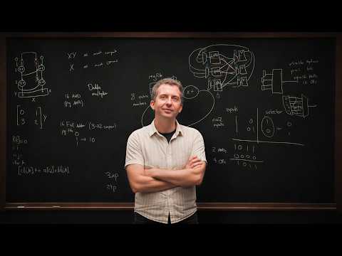
“So this circuit I’ve described here, almost all of the cost, like uh, seven-eighths of the cost, is in the reading and writing the register file, and only a tiny fraction of the cost is in the logic unit itself. So this is the problem to solve.” — Reiner Pope, 25:05
Clip command
yt-dlp --download-sections "*25:05-26:00" "https://www.youtube.com/watch?v=oIk3R-sMX5o" --force-keyframes-at-cuts --merge-output-format mp4 -o "register-file-tax.mp4"”The key trick is that this matrix can be stored locally to the systolic array”
“And so instead we’re going to store, our key trick is that this matrix can be stored locally to the systolic array.” — Reiner Pope, 29:56
Clip command
yt-dlp --download-sections "*29:22-30:30" "https://www.youtube.com/watch?v=oIk3R-sMX5o" --force-keyframes-at-cuts --merge-output-format mp4 -o "systolic-trick.mp4"”An FPGA is an order of magnitude more expensive than an ASIC”
“And so I mean one of the things you can do here is you can see why the rule of thumb that an FPGA is like an order of magnitude more expensive than an ASIC comes from is to count how many gates would be inside this lookup table.” — Reiner Pope, 58:50
Clip command
yt-dlp --download-sections "*58:50-1:00:00" "https://www.youtube.com/watch?v=oIk3R-sMX5o" --force-keyframes-at-cuts --merge-output-format mp4 -o "fpga-10x-asic.mp4"”Inside the CPU, very little is actually the ALUs”
“Inside the CPU you have so one big use of area in a CPU are the cache. Very little is actually the ALUs, like mostly it’s like these register files rather than the logic units… But the thing that does not have an equivalent in a GPU is the sort of this branch predictor. And so there is a whole big area in the CPU which is sort of just a whole bunch of predictors.” — Reiner Pope, 1:09:13
Clip command
yt-dlp --download-sections "*1:09:00-1:10:30" "https://www.youtube.com/watch?v=oIk3R-sMX5o" --force-keyframes-at-cuts --merge-output-format mp4 -o "cpu-branch-predictor.mp4"”Most of the energy is consumed in toggling bits from zero to one and back”
“Most of the energy consumption actually comes from just the charging and discharging of like toggling from zero to one and back to zero. So if you run a chip much slower and you only clock it once every thousand clock cycles, you will have a thousand times fewer transitions. It’ll be about a thousand times less energy consumption, but not a substantial advantage in energy efficiency.” — Reiner Pope, 1:15:00
Clip command
yt-dlp --download-sections "*1:14:47-1:15:30" "https://www.youtube.com/watch?v=oIk3R-sMX5o" --force-keyframes-at-cuts --merge-output-format mp4 -o "chip-energy-toggling.mp4"”A GPU is just a bunch of tiny TPUs”
“You can sort of think of taking scaling this thing down into a really tiny unit with a smaller matrix unit, smaller vector unit and that is sort of what an SM is. So, sort of at a very high level point of view, the GPU has a lot of tiny tiny TPUs sort of tiled across the whole whole chip.” — Reiner Pope, 1:15:31
Clip command
yt-dlp --download-sections "*1:15:31-1:17:30" "https://www.youtube.com/watch?v=oIk3R-sMX5o" --force-keyframes-at-cuts --merge-output-format mp4 -o "gpu-tiny-tpus.mp4"Key Points
- Multiply-accumulate is the atomic operation of a matrix multiply (0:54) - For loop over I, J, K: output[I,K] += input[I,J] * input[J,K]. Every step is one MAC
- The Dadda multiplier compresses partial products with full adders (10:17) - A full adder is a “three-to-two compressor”; standard way to build multipliers
- Why the multiplication step is low-precision and the accumulation step is higher precision (2:39) - Errors accumulate quickly during the sum, so you need more bits there. This is also why NVIDIA reports 4-bit ops as 2x not 4x of 8-bit ops — the adder doesn’t scale quadratically
- Quadratic die-area scaling with bit precision (14:44) - A multiplier grows roughly quadratically with bit width, so FP4 should be ~4x faster than FP8 by area. NVIDIA’s older specs reported 2x; B300 finally acknowledges ~3x. Should be 4x
- The mux is a hidden data-movement cost (18:51) - Selecting one register out of n requires ANDs and ORs that scale as n*p (rows times bits). Seven-eighths of total gate cost
- Systolic array bakes a whole matrix loop into hardware (25:59) - Bigger fixed-function units amortize the input/output tax. The weight matrix stays fixed locally for many cycles while activations stream through
- Pipeline register insertion is a major chip-design task (43:43) - Chip architects set the clock cycle; tools place registers to balance paths so signals arrive synchronously
- FPGAs vs ASICs (51:40) - An FPGA is a sea of 4-input lookup tables (LUTs) you program “in the field” (deployed in a data center) by configuring muxes
- A 4-input LUT can implement any of 16 different functions (57:34) - Truth table with 16 rows; you can program any logic gate. Sweet spot for FPGA design
- Why FPGAs are ~10x more expensive than ASICs (58:50) - A LUT is ~32 gates to implement what 3 AND gates would do directly in an ASIC. The mux + LUT overhead is the cost of flexibility
- Cache vs scratchpad (1:03:14) - CPU caches: hardware decides what to keep based on access patterns. TPU/GPU scratchpads: software issues an explicit instruction to load from HBM/DDR
- Why CPU cores are much bigger than GPU cores (1:09:13) - The branch predictor occupies a huge area in a CPU; GPUs strip it out
- A GPU is just a bunch of tiny TPUs (1:15:22) - TPUs have a few large matrix units; GPUs have a regular grid of SMs, each of which is a small matrix unit + vector unit
- Tradeoff: TPU amortizes better; GPU has more vector-matrix bandwidth (1:18:21) - GPUs move data across many lines of perimeter between vector and matrix units; TPUs move it through just two
- MatX is building a “splittable systolic array” (1:20:08) - Hybrid that captures GPU’s smaller-grain flexibility within a TPU-like larger systolic structure
- Chip energy ≈ dynamic switching power (1:14:47) - Most energy goes into charging and discharging capacitors during bit transitions. Running the chip 1000x slower → 1000x less switching → 1000x less energy, but no efficiency advantage per op
- Brain-vs-chip clock speed gap doesn’t yield 1000x energy advantage (1:13:05) - A slower clock saves energy in proportion to the slowdown, not exponentially
- Brains co-locate memory and compute (1:12:18) - But Pope notes systolic arrays do this too — weights are stored in the array
Mentions
Companies
- MatX (0:00) - Reiner’s new AI chip startup; Dwarkesh is an angel investor
- NVIDIA (12:42) - Reference for FP4 vs FP8 specs; B100/B200/B300 generations; Volta as the moment they baked multiply-accumulate into hardware
- Google / TPU team (25:21) - Where Reiner previously worked; TPU is the running architectural comparison
- TSMC (48:29) - Provides PDK with primitives (AND gates, full adders) for chip designers
- Crusoe (21:29) - Sponsor; gold-tier GPU cloud in SemiAnalysis ClusterMAX report
- Cursor (37:54) - Sponsor; Dwarkesh used it for essay-contest review interfaces
- Jane Street (49:38) - Sponsor; Ron Minsky and Dan Pontecorvo on hiring engineers, signed $6B compute deal
- SemiAnalysis (21:29) - Cloud Spectator and ClusterMAX reports referenced
- AMD (1:01:34) - Maker of FPGAs (Xilinx); opinionated wiring layouts
Products & Technologies
- Multiply-accumulate (MAC) (0:54) - The atomic chip-level primitive for matrix multiply
- AND/OR gates and full adders (0:33) - The smallest building blocks; everything compiles down to these
- Dadda multiplier (10:17) - Standard chip-design pattern for combining partial products
- Multiplexer (mux) (18:00) - The cost of selecting one of n inputs; ubiquitous and expensive
- Systolic array (25:59) - Bake a whole loop into hardware; weights stored locally
- Pipeline registers (45:21) - Inserted along data paths to keep clock cycles short
- FPGA / LUT (lookup table) (51:40) - Field-programmable gate array; 4-input LUTs implement any 4→1 function
- ASIC (51:40) - Application-specific integrated circuit; the cheap, fast comparison
- PDK (process design kit) (47:03) - TSMC’s library of timing-characterized primitives
- Cache (CPU) (1:03:14) - Hardware-managed memory hierarchy; 2 orders of magnitude faster than DDR
- Scratchpad (TPU/GPU) (1:06:56) - Software-managed local memory; deterministic latency
- HBM (high bandwidth memory) (1:06:32) - Off-chip memory for TPUs/GPUs
- DDR memory (1:04:37) - Off-chip memory for CPUs
- Branch predictor (1:10:14) - Big CPU subsystem that guesses which way conditional branches will go
- SM (Streaming Multiprocessor) (1:16:00) - The repeating GPU compute tile; functionally a tiny TPU
- MXU (Matrix Unit) (1:17:25) - The large TPU systolic array; analogous to a GPU’s tensor core
- Splittable systolic array (1:20:08) - MatX’s public design direction
- FP4 / FP8 / BF16 (13:54) - Floating-point formats; precision-vs-throughput tradeoff
- Volta GPU generation (25:21) - When NVIDIA first baked MAC into hardware via tensor cores
People
- Reiner Pope (0:00) - CEO of MatX, former TPU architect at Google; the lecturer
- Clark (Jane Street FPGA engineer) (51:40) - Helped Dwarkesh prep for the previous Reiner Pope episode
- Ron Minsky (49:38) - Senior Jane Street, in sponsor segment about AGI-complete trading
- Dan Pontecorvo (49:38) - Runs Jane Street’s physical engineering team
- John von Neumann (1:07:18) - Architecture namesake; Dwarkesh asks whether modern chips even fit the “serial fetch/decode/execute” picture
Surprising Quotes
“It’s muxes all the way down.” — Reiner Pope, on FPGA architecture, 1:00:09
“Most of the decisions in chip design are sizing decisions.” — Reiner Pope, 36:42
“The throughput of your chip you can think of as the product of how much do I get done per clock cycle times how fast my clock is.” — Reiner Pope, 49:13
“Trading in particular feels to me as like kind of AGI complete, sort of like NP complete.” — Reiner Pope (in sponsor segment quote), 51:00
“Field as in like out there in the world field.” — Reiner Pope, clarifying what “field-programmable” actually means, 55:41
Transcript
Dwarkesh Patel: 0:00 I’m back with Reiner Pope who is the CEO of MatX, which is a new AI chip company. Last time we were talking about what happens inside a data center. Now I want to understand what happens inside an AI chip. How does a chip actually work? Full disclosure, by the way, I am an angel investor in MatX, so hopefully you have designed a good chip.
Reiner Pope: 0:20 So I’ll start with sort of the very smallest fundamental unit of chip design and then we’ll sort of build up into what an overall like actual production chip, what are the components of that. At the very bottom level of a chip, the primitives that we work with are logic gates, which are very simple things like AND, OR, NOT, and then these are connected together by wires that have to be laid out physically as metal traces on a chip. The main function that AI chips want to compute is multiplication of matrices and really inside that the fundamental primitive is multiply-accumulate just like of pairs of numbers. So we’re going to demonstrate what that calculation looks like by hand and then sort of infer what a circuit would look like for that. It’ll turn out to be easiest if I do multiplication-accumulate of something like a four-bit number with another four-bit number, and then the actual clearest primitive is multiply-accumulate — so multiply these two terms and then add in an eight-bit number.
Dwarkesh Patel: 1:45 Can I ask a clarifying question? Why is this the natural primitive for whatever computation happens inside a computer?
Reiner Pope: 1:51 Yeah, so there’s a few reasons for this. It’s a little bit more efficient but the reason it’s natural for AI chips is that if you look what’s happening during a matrix multiply, the — what is matrix multiply in very short? It is a for loop over I and over J and over K of output[I,K] += input[I,J] times other input[J,K]. And so multiply-accumulate happens at every single step of a matrix multiply.
Dwarkesh Patel: 2:38 Makes sense.
Reiner Pope: 2:39 And then the other observation is that the precision will almost always be higher in the accumulation step than in the multiplication step. This is maybe specific to AI chips but you’re multiplying low precision numbers but then when you accumulate errors accumulate quickly and so you need more precision here. So this is why we’ve chosen to do a four-bit multiplication and an eight-bit addition.
Dwarkesh Patel: 3:00 There’s two ways to understand that, one is that the value will be larger than the inputs, and the other is that if it was a floating point number it would be maybe — that part is less intuitive to me, but it’s maybe the same principle.
Reiner Pope: 5:11 So firstly, what logic gates did it take us to even get to this intermediate step? We needed to produce all 16 of these partial products. How do I produce one of these partial products? Let’s take this number one for example here, it is one, so we can actually produce that by an AND gate — this number is one if both this bit is one and this bit is one. If either is zero, output zero. Then this will be P times Q many ANDs. Finally I sum them. Actually, most of the work is going to happen in the summing. So let me describe a full adder. What this does is, coming from software, you might think that a full adder adds 32-bit numbers, but here it’s a three-to-two compressor because it takes three bits of input and produces two bits of output.
Dwarkesh Patel: 7:21 The two inputs are an X and a Y value and then some carry that came in from —
Reiner Pope: 7:31 Sorry, the three inputs are all bits that are in the same sort of bit position, like three bits that are in the same column.
Dwarkesh Patel: 8:04 So if the inputs in the full adder are, let’s say, 1-0-1, then the output will still be 1-0. If it was 1-1-1, it’d be 1-1.
Reiner Pope: 8:22 So this circuit actually can sort of capture what we as humans naturally do when we’re doing summing algorithms. Same thing with this column, we’ve got a column of one, two, three, four numbers, and so maybe we’ll take the first three and put them through a full adder. Let’s just keep going a little more — I take these three numbers, I add them, that gives me a one and a zero. So the way I should view this is that I have this whole grid of numbers that need to be added. I’m going to keep compressing them down three at a time. This approach is called a Dadda multiplier, and it’s sort of like the standard chip-design pattern.
Reiner Pope: 10:34 Let’s try and quantify the circuit size of this just so we’ve got a sense of how big things are so we can compare to other things. And then on I produced eight bits on the output eventually. And in every step I was sort of crossing off three numbers and adding back two.
Dwarkesh Patel: 11:38 Let me just make sure I understand the logic of that. So the input bits are P times Q plus P plus Q.
Reiner Pope: 11:47 That’s right.
Dwarkesh Patel: 11:48 And the output bits is just P plus Q. And so P times Q plus P plus Q minus P plus Q equals P times Q.
Reiner Pope: 11:58 That’s right. So this hints at the second reason why we chose to do a multiply-accumulate. So we’ve described this whole procedure, every single atomic step that I took here becomes a logic gate.
Dwarkesh Patel: 12:42 This may be the wrong time to ask this question, but whenever NVIDIA reports that this chip can do X many FP4 or half as many FP8 — are these actually the same circuits doing both?
Reiner Pope: 13:31 As drawn, they’re actually not particularly fungible. This is actually one of the main choices you have to make when you design a chip.
Dwarkesh Patel: 13:54 But so then when they report those numbers and they just happen to be the case that it does 2x as many FP4 as FP8, what’s going on?
Reiner Pope: 14:12 Yeah, so part of it is, that surely won’t be exactly equivalent die area. There’s a data movement thing.
Dwarkesh Patel: 14:44 Actually, come to think of it, it’s not just 2x — the amount of area it takes sounds like it’s quadratic in the bit precision.
Reiner Pope: 15:03 So, in fact NVIDIA made a change. Historically, up until B100 or B200 every time you halved the bit precision you doubled the throughput.
Dwarkesh Patel: 15:17 That ratio is exactly like for the reason you said, because of this quadratic scaling that ratio is actually slightly wrong.
Reiner Pope: 15:27 NVIDIA’s product specs have sort of started acknowledging that in B300 and beyond where the FP4 is three times faster.
Dwarkesh Patel: 15:39 Though it should be 4x.
Reiner Pope: 15:40 Yeah. What I’ve shown here is the simplest case of integer multiply. When you’re dealing with floating point it’s a little different.
Dwarkesh Patel: 15:54 So what can we see already from this? I think the big observation you’ve made is that there’s this quadratic scaling.
Reiner Pope: 16:12 But the other thing we’re going to do now is compare the area spent on the multiplication itself with all the circuitry around it — like the muxes for reading and writing registers. Just like this guy, I might select any of the registers at any point in time. A first question is, how costly is that? And what is the cost of this thing? All we have to build it out of is AND and OR.
Dwarkesh Patel: 18:51 Okay, just to make sure I understand the basics. What the MUX is doing is just selecting an input.
Reiner Pope: 18:58 Yeah, so invisible to software, it’s like you say “I want input number three,” that means there’s a MUX. So what is the cost of this MUX? An n-input MUX operating on p bits — every single input, I have to say, am I going to mask it out or not? And then I’m going to OR them all together.
Dwarkesh Patel: 19:58 Got it. It’s actually kind of funny that you would sort of — you don’t think at the level of hardware about how much it costs to even pick which input.
Reiner Pope: 20:14 Yeah, this is the first step of all of the hidden data movement costs that show up. If we plug in actual numbers, like n being eight, I get like twenty-four times p gates over just the adder, multiply-adder.
Dwarkesh Patel: 21:29 In the most recent Cloud Spectator report, SemiAnalysis ranked almost 100 different GPU clouds. Crusoe was one of only five that made gold tier.
Dwarkesh Patel: 22:43 It might be helpful to just see what a mux looks like, maybe like a two-bit or a four-bit mux.
Reiner Pope: 22:48 Great. So we’ll take some inputs, we’ll have a two-way mux. We’ve got two different inputs. We just want to produce this guy as the result. And so very laboriously we AND this and OR these together.
Reiner Pope: 25:05 So this circuit I’ve described here, almost all of the cost — seven-eighths of the cost — is in the reading and writing the register file, and only a tiny fraction of the cost is in the logic unit itself. So this is the problem to solve. This essentially was the state of play prior to the Volta generation of NVIDIA GPUs.
Reiner Pope: 25:59 The evolution was: we had baked this much into hardware in this stage. This single line is a multiply-accumulate and this single thing was baked into hardware. The idea of a systolic array is to go two levels of loop up and bake this entire loop into hardware. If we have a much bigger granularity fixed-function piece of logic, maybe the taxes we pay on the input and output are much smaller.
Dwarkesh Patel: 26:30 It sounds like you’re suggesting that if you go up one step in the matrix-multiply loop, then there’s some quantity that stays fixed.
Reiner Pope: 26:44 That’s right. There’s two effects we’re going to take advantage of. One is just that we can do more steps with some things staying fixed. Visually we’re going to look at this matrix multiplication. This portion of the loop corresponds to a matrix-vector multiply. We take every column, get multiplied by the vector, and then summed. There is a multiplier-accumulate associated with every single one of these entries in the matrix.
Reiner Pope: 29:11 However, we need to somehow manage the communication of this matrix which exceeds our budget of x. And so the idea is that in an AI context, this matrix is actually going to stay fixed for a long period of time. And so instead of bringing it in from the outside — we’ve got some register file sitting over here — we don’t want to bring this full matrix in from the register file every cycle because we don’t have enough bandwidth. Instead we’re going to store — our key trick is that this matrix can be stored locally to the systolic array. And so we’ll store these numbers 0, 1, 2, and 3 in a gate called a register that physically stores these numbers and we’re going to reuse these numbers many cycles.
Dwarkesh Patel: 30:22 And so the optimization here is that the nature of matrix multiplication is you can store this like square or quadratic-sized matrix in the systolic array and only stream the vector through.
Reiner Pope: 30:44 That’s right. This is the nature of what a matrix multiplication is — you do a lot of multiplication to get the output relative to the size of the input.
Reiner Pope: 33:00 The weight matrix is stored locally in systolic array, but we just do it very slowly. We trickle-feed it into the systolic array.
Dwarkesh Patel: 34:23 I see. So there’s two questions in terms of communication. There’s communication time and then there’s communication amortization.
Reiner Pope: 34:46 Exactly.
Dwarkesh Patel: 34:50 Interesting. So it’s interesting that when we were talking last time about inference across many chips the big highlight was that the network communication had to be — exactly the same point.
Reiner Pope: 35:18 This turns up all the way up and down the stack. This is close to the bottom — the systolic array. The systolic array I drew it as 2x2, but in older TPUs they would describe it as 128 by 128.
Dwarkesh Patel: 36:21 I see. So we’ve talked about how it seems obvious that you should try to maximize compute relative to communication.
Reiner Pope: 36:42 Most of the decisions in chip design are sizing decisions.
Dwarkesh Patel: 37:54 [Cursor sponsor segment]
Dwarkesh Patel: 39:00 Where does the clock cycle of a chip come in and what determines what that is? What is a clock cycle of a chip?
Reiner Pope: 39:09 At baseline, it’s worth observing that chips are incredibly parallel. So that is the clock cycle. The entire chip typically all in one fell swoop goes in lockstep to the next operation. There is a global clock signal which drives all of these registers. It says at a certain instant in time when the clock ticks, registers update.
Reiner Pope: 41:38 A major point of optimization on any chip then is to make this delay — the delay from here to here — as short as possible.
Dwarkesh Patel: 41:51 Interesting. So because the constraint here is that if you add too much logic, then you might risk missing the clock cycle. But if you don’t add enough, then you’re not using the chip’s full capacity.
Reiner Pope: 42:24 In standard chip design, there is a probability of missing a cycle, but it’s like many, many standard deviations away.
Dwarkesh Patel: 42:58 And the clock where the registers are — this is not something you determine when designing the layout?
Reiner Pope: 43:43 Yeah, this is a huge part of the work of designing a chip — inserting them. So it is done in an automated way.
Dwarkesh Patel: 44:22 Stepping back, why do we need to synchronize the whole chip? Like if you imagine playing Factorio, you have a bunch of factories and they don’t need to be synchronized.
Reiner Pope: 44:35 Taking that analogy, the thing you need to be mindful of is if I’ve got two different paths — F will take a little longer maybe in some chips, G will take a little bit longer. And so if I’ve got some signal that combines these.
Dwarkesh Patel: 45:18 And H needs to know when to start.
Reiner Pope: 45:20 Exactly.
Dwarkesh Patel: 45:21 Like when has this next iteration — and so this explains why different chips made at the same process node can have different clock speeds.
Reiner Pope: 45:51 That’s right. This optimization I showed here, this is pipeline register insertion.
Dwarkesh Patel: 47:03 And I guess it’s then up to — so TSMC offers a PDK which says, hey, here’s the primitives of logic that we can grant you.
Dwarkesh Patel: 48:00 And in the chip, it’s up to them to determine that no primitive is bigger than the clock cycle they’re hoping for.
Reiner Pope: 48:23 As a logic designer, like the chip architects set the clock cycle. The primitives you get from TSMC are on the order of AND gates or full adders. They depend a lot on voltage and frequency.
Dwarkesh Patel: 49:03 Interesting. So what you’re hinting at is a dynamic where you can have really fast clock speed, but you’re not getting throughput.
Reiner Pope: 49:13 Or throughput rather. The throughput of your chip you can think of as the product of how much do I get done per clock cycle times how fast my clock is.
Dwarkesh Patel: 49:38 [Jane Street sponsor segment - language models competing against best human forecasters]
Reiner Pope: 49:50 There’s a world that we should take seriously where we’re going to build large language models or some other AI capable at all cognitive tasks. Trading in particular feels to me as like kind of AGI complete, sort of like NP complete.
Dwarkesh Patel: 51:40 Okay, so I remember talking to an FPGA engineer at Jane Street, Clark, who actually helped me prep for your previous episode. What’s the difference between an FPGA and an ASIC?
Reiner Pope: 52:24 Yeah, so firstly let’s consider the business case for an FPGA versus an ASIC. These are called LUTs — look-up tables — which actually provide all of the gates.
Dwarkesh Patel: 54:07 And then we’re going to see in the sort of the third component, we then have a swarm of these LUTs.
Reiner Pope: 54:27 Muxes. So in front of every single one of these we’ve got something like one of these muxes which selects one input from a bunch of nearby registers.
Dwarkesh Patel: 54:53 So what this allows is essentially, when I program my FPGA I can say that I’m going to take all of these components and program in.
Dwarkesh Patel: 55:31 What does it mean to be programmed into a field?
Reiner Pope: 55:34 Programmed in the field — the device has been deployed in a data center, it’s sitting in the field, and then you can reprogram it.
Dwarkesh Patel: 55:39 Not field as in like electromagnetic field?
Reiner Pope: 55:41 Field as in out there in the world field.
Dwarkesh Patel: 55:43 And so if I see how the field programming comes out of the first lookup table and goes into a second one.
Reiner Pope: 55:55 I got a little bit lazy in drawing all of these. Every single device here has a mux sitting in front of it. Programming it consists of configuring every single one of these muxes.
Dwarkesh Patel: 56:47 So that makes sense. What is happening inside the lookup table?
Reiner Pope: 56:51 The purpose of the lookup table is to be able to configurably take the role of an AND gate, OR gate, XOR, any of those different things.
Dwarkesh Patel: 57:30 How many different functions are there from four bits to one bit?
Reiner Pope: 57:34 There are 16 different functions. And so you can actually just tabulate this as 16 different numbers.
Dwarkesh Patel: 58:13 Okay, so the lookup table — if you think about an NAND gate, OR gate, NOR gate, XOR gate — these are all like take as input two-bit functions.
Reiner Pope: 58:21 Those are two-input functions. Sometimes we have more complicated, like a three-input function.
Dwarkesh Patel: 58:31 Typical size for LUTs is four input?
Reiner Pope: 58:31 Typical size for LUTs is four input, which is a sweet spot.
Dwarkesh Patel: 58:43 But basically the lookup table is like a truth table.
Reiner Pope: 58:45 It’s a truth table.
Dwarkesh Patel: 58:46 And with a truth table you can program in any gate you want.
Reiner Pope: 58:50 That’s right. And so one of the things you can do here is you can see why the rule of thumb that an FPGA is like an order of magnitude more expensive than an ASIC comes from — count how many gates would be inside this lookup table. We can view this lookup table essentially as one of these muxes and so it is a mux which has to select between 16 different rows.
Dwarkesh Patel: 59:50 This circuit being the mux?
Reiner Pope: 59:52 Yeah exactly, the mux. The lookup table itself you can think of as actually a big mux that selects from all 16 rows down to one output.
Dwarkesh Patel: 1:00:03 Yeah, okay. That is the lookup table. But the way you’ve drawn it here, there’s like a mux and then a lookup table.
Reiner Pope: 1:00:09 It’s muxes all the way down — there’s a second mux that is inside here.
Dwarkesh Patel: 1:00:14 Got it. And then the other mux is just saying where it came from in this sort of mess of gates.
Reiner Pope: 1:00:21 Right. And then the second mux is, okay, now you have one value, but that value is still a 4-bit value. So I’ve selected four bits from the soup. And then I use those four bits to select which entry in the lookup table.
Dwarkesh Patel: 1:02:15 Right. And the reason it’s 10x slower is why?
Reiner Pope: 1:02:18 If you look at the cost of building this lookup table, it’s like 32 gates. And then it can give me the equivalent of three AND gates. So the overhead is really coming from the fact that the lookup table — the mux and the lookup table together — are listing out every single possible combination of input.
Dwarkesh Patel: 1:03:13 Interesting. One important point you made to me is that the reason they prefer FPGAs to CPUs is because they get deterministic latency.
Reiner Pope: 1:03:27 You can actually design a CPU that has deterministic latency as well. In a CPU you have the CPU die itself, and then there’s a memory off on the side. This is the DDR. The cache is two orders of magnitude faster than the DDR. If you never line up well with the cache, you take this big penalty. The big thing that you can do differently is instead of having the hardware say “I’m going to read memory and then decide” — the hardware decides whether or not — a different design philosophy is, you see this in TPUs for example, the TPU instead has a scratchpad.
Reiner Pope: 1:06:32 So the main difference is this would be like a TPU and then HBM in this case rather than DDR but it’s still an off-chip memory. And instead of like the software saying “first access memory and then the hardware decides,” you’ve got some instructions in software.
Reiner Pope: 1:06:56 So this style is generically known as scratchpad instead of cache. The key distinction being that you have one explicit instruction to load.
Dwarkesh Patel: 1:07:11 So it’s scratchpad being the cache.
Reiner Pope: 1:07:13 This thing here is the scratchpad.
Dwarkesh Patel: 1:07:18 So stepping way back, people say computers have the John von Neumann architecture where there’s this serial fetch/decode/execute. Even CPUs are super parallel if you think about all the cores they have. In what sense is modern computing even von Neumann?
Reiner Pope: 1:07:52 I think it’s a fair way to describe CPUs. The amount of parallelism on a CPU is small.
Dwarkesh Patel: 1:08:08 I guess one question is, what is being used for the CPU, and if there’s fewer threads, why does CPU have so few cores?
Reiner Pope: 1:08:38 The cores are just much bigger and more complicated.
Dwarkesh Patel: 1:09:00 Like why are there more CUDA cores, for example, than CPU cores?
Reiner Pope: 1:09:13 Inside the CPU you have one big use of area — the cache. Very little is actually the ALUs, mostly it’s like these register files rather than the logic units. Both of these things have equivalents in a GPU. But the thing that does not have an equivalent in a GPU is the branch predictor. There is a whole big area in the CPU which is just a whole bunch of predictors that are saying when will my next branch be and where’s the branch target for that? Stripping a lot of that out as well as making these register files tighter is driving a lot of the GPU gains.
Dwarkesh Patel: 1:10:08 And what is the purpose of the branch predictor? To execute both branches at once or what does it do?
Reiner Pope: 1:10:14 The issue is that when I’ve got a series of instructions, like instruction, instruction, instruction, instruction — I issue them one at a time. But while one is in flight I want to start on the next.
Dwarkesh Patel: 1:11:50 So if I think about how the brain works versus what you’re describing here, at a high level, the differences might be that while you can do structured sparsity in these accelerators — and then save yourself some area that you would have otherwise had to dedicate to these gates. In the brain, there’s unstructured sparsity. Then there’s the fact that memory and compute are co-located.
Reiner Pope: 1:12:17 Yeah.
Dwarkesh Patel: 1:12:18 I guess you could say in a way the memory and compute co-located.
Reiner Pope: 1:12:23 This is exactly the co-location in some sense of the memory. That’s right.
Dwarkesh Patel: 1:12:27 So maybe that actually isn’t a big difference. And the other maybe a bigger difference is that the clock cycle on the brain is much, much slower.
Reiner Pope: 1:13:05 Let’s take the clock speed one first. The clock speed is quite high on a chip because that drives high throughput. When we compare a GPU running some workload, it’s running batch size 1000. The brain is not running batch size 1000. There’s only one of me. You could imagine: take a GPU and instead of running it at a gigahertz, run it at a megahertz, and that would start to look maybe a little bit more like equivalent things in the brain. In the way silicon works, that does not give you a thousand-x advantage in energy efficiency. What it ends up looking like is you can run this circuit once to stabilization and then it’ll sit idle for a long period of time. It doesn’t consume a lot of energy while sitting idle because most of the energy is consumed in toggling bits from zero to one and back. The way to think of a bit being stored is you’ve effectively deposited some charge in a capacitor. So it becomes charged when it becomes a one and discharged when it next goes to a zero. That cycle of charging and dumping that charge out to ground, that is where the energy is consumed.
Reiner Pope: 1:14:47 This is called the dynamic or switching power, this is most of the energy consumption of a chip. There is some other energy consumption.
Reiner Pope: 1:15:00 Most of the energy consumption actually comes from just the charging and discharging of toggling from zero to one and back to zero. So if you run a chip much slower and you only clock it once every thousand clock cycles, you will have a thousand times fewer transitions. It’ll be about a thousand times less energy consumption, but not a substantial advantage in energy efficiency.
Dwarkesh Patel: 1:15:23 Okay, so you’ve described how a TPU works at a high level. What is the difference at a high level between how a GPU and a TPU work?
Reiner Pope: 1:15:31 There’s a high-level organization principle that is different. We’ll look at outside the core, at the high level. If you think of this as the whole chip in each case, the organization of the GPU is mostly a bunch of almost identical units which are the SMs. They’ve got an L2 memory in the middle and then a bunch more SMs on the bottom. So there’s a fairly regular grid of cores. If we look at a TPU in comparison, you end up with much coarser-grained units of logic — a large number of, maybe just a few, matrix units (the big systolic arrays) and in the middle you’ve got some vector unit and your matrix units at the bottom. So you can think of taking this and scaling it down into a really tiny unit with a smaller matrix unit, smaller vector unit, and that is sort of what an SM is. So at a very high level, the GPU has a lot of tiny tiny TPUs sort of tiled across the whole chip.
Dwarkesh Patel: 1:17:25 Oh interesting. So you’re suggesting the tensor core within a streaming SM is analogous to an MXU?
Reiner Pope: 1:17:35 Yeah, it’s very very similar.
Dwarkesh Patel: 1:17:37 I see. So if you had more lack of structure, having a bunch of tiny TPUs makes a lot of sense, whereas if you’ve got a lot of structure, the TPU is better.
Reiner Pope: 1:18:00 Across the whole thing. I think this shows up in how large you can grow things. Especially with a systolic array, a larger systolic array amortizes the register file costs better. This design allows you to have larger systolic arrays, whereas the GPU design constrains you to have small units of everything.
Reiner Pope: 1:18:21 There is a trade-off, however. Because of this coarse-grained separation of things, you need to move a lot of data from the vector unit to the matrix units. So you need to move a lot of data through two lines of perimeter here. Whereas if you look at the equivalent thing here, you’ve got vector units everywhere, and you need to move data through this line, through this line, through this line, through this line, through this line, through this line. So the amount of data you can move between a vector unit and a matrix unit is actually much higher in a GPU than in a TPU because instead of having to move all the data through these just two lines, you’re moving all the data through like 16 lines of wiring in a GPU.
Dwarkesh Patel: 1:19:17 Right, but also you might have to move across less area.
Reiner Pope: 1:19:22 Which is also a saving, an energy saving. So data ends up moving — if you can operate entirely within a single SM, you’ve saved a lot of energy.
Dwarkesh Patel: 1:19:37 So you didn’t comment, but one might expect that a thing MatX might try to do is to get the GPU-like smaller structure while keeping TPU’s larger systolic amortization.
Reiner Pope: 1:20:08 Yeah. We’ve talked publicly about something which we call a splittable systolic array, which is sort of in some sense exactly that.
Dwarkesh Patel: 1:20:17 Cool. Okay, I think this is a good note to close on. Reiner, thank you so much.
Reiner Pope: 1:20:23 Thanks, Dwarkesh.